Market Overview
The global Advanced Packaging Chemicals Market includes specialty process chemicals, polymeric materials, plating chemistries, dielectric materials, cleaning chemicals, bonding materials, underfills, encapsulants, temporary bonding materials, debonding chemistries, surface preparation materials, post-patterning cleans, and thermal management materials used in advanced semiconductor packaging. The market covers chemicals and materials used in fan-out wafer-level packaging, flip chip, FCBGA, 2.5D interposer packaging, 3D stacking, high-bandwidth memory, chiplets, hybrid bonding, redistribution layers, through-silicon vias, copper pillars, micro-bumps, wafer thinning, and package-level interconnect formation. It excludes conventional commodity packaging consumables, standard board-level assembly materials, and general electronics chemicals not used in advanced semiconductor packaging workflows.Advanced packaging chemicals are becoming strategically important because package architecture is now a direct path to performance improvement. As front-end scaling becomes more expensive, chipmakers are using chiplets, 2.5D interposers, HBM stacks, fan-out structures, and hybrid bonding to improve bandwidth, power efficiency, form factor, and system-level integration. SEMI reported that global 300mm fab equipment spending is expected to rise 18.0% to US$ 133.0 billion in 2026 and 14.0% to US$ 151.0 billion in 2027, supported by AI chip demand, data centers, edge devices, and regional semiconductor self-sufficiency programs. This fab investment cycle strengthens demand for advanced packaging materials because AI and high-performance computing devices increasingly require complex back-end integration.
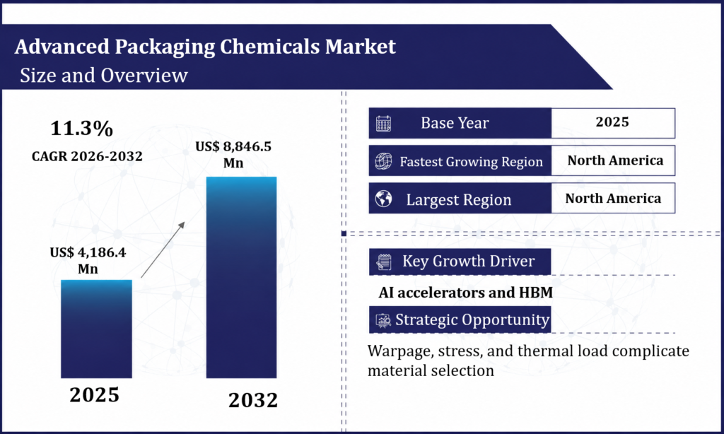
The global Advanced Packaging Chemicals Market was valued at US$ 4,186.4 million in 2025 and is projected to reach US$ 8,846.5 million by 2032, registering a modeled CAGR of 11.3% during 2026-2032.
Growth is being driven by HBM integration, AI accelerators, chiplet architectures, advanced substrates, hybrid bonding, fan-out packaging, copper redistribution layers, and increasing demand for packaging-level yield control. Unlike traditional packaging materials, advanced packaging chemicals are selected not only for mechanical protection, but also for interconnect reliability, surface cleanliness, thermal stability, warpage control, low ionic contamination, and compatibility with fine-pitch structures.
The market’s structure is being shaped by two overlapping material needs. First, packaging processes require high-purity chemicals for plating, cleaning, etching, residue removal, surface activation, and bonding preparation. Second, advanced packages require engineered polymers, underfills, encapsulants, dielectric films, temporary bonding layers, release materials, and thermal materials. Merck states that its packaging offering spans the advanced packaging value chain with thick film resists, packaging cleans, slurries, and interconnect materials, showing how packaging has become a multi-chemistry platform rather than a single materials category.
The strongest structural shift is the movement from package protection to package-enabled computing. HBM, 2.5D interposers, fan-out packages, and chiplet systems require materials that can survive thinner die, tighter interconnect pitch, larger package body sizes, higher thermal load, and mixed coefficients of thermal expansion. Henkel describes advanced packaging materials such as thermal interface materials and underfills as important to semiconductor package performance, with underfills filling gaps between the silicon die and substrate to protect chips from heat and physical stress.
Executive Market Snapshot
| Metric | Value |
| Market Size in 2025 | US$ 4,186.4 million |
| Market Size in 2032 | US$ 8,846.5 million |
| CAGR 2026-2032 | 11.3% |
| Largest Product Type in 2025 | Underfills, Encapsulants and Mold Compounds |
| Fastest-Growing Product Type | Hybrid Bonding Surface Preparation Chemicals |
| Largest Application in 2025 | Flip Chip and FCBGA Packaging |
| Fastest-Growing Application | High-Bandwidth Memory and AI Accelerator Packaging |
| Largest End Use in 2025 | OSAT Providers |
| Fastest-Growing End Use | Memory Manufacturers |
| Largest Region in 2025 | Asia-Pacific |
| Fastest Strategic Growth Region | North America |
| Most Important Country Opportunity | Taiwan |
| Highest Strategic Priority Theme | Materials reliability for chiplet, HBM, and heterogeneous integration |
Analyst Perspective
The Advanced Packaging Chemicals Market should be interpreted as a reliability-enabling materials market rather than a back-end consumables market. The role of packaging chemicals has expanded from protecting the die to enabling electrical performance, thermal dissipation, mechanical stability, and system integration. In AI accelerators, HBM packages, and chiplet-based devices, the package is no longer a passive enclosure. It is an active performance architecture, and chemicals determine whether redistribution layers, micro-bumps, bonding surfaces, dielectrics, underfills, and encapsulants can operate reliably at scale.The most attractive value pool is forming around fine-pitch interconnects and high-density integration. Redistribution layers, copper pillars, TSVs, micro-bumps, and hybrid bonding structures require plating chemistry, wet cleans, surface activation chemicals, dielectric materials, and residue control systems with very narrow process windows. Small variations in surface contamination, ionic residues, copper roughness, polymer cure, or underfill flow can reduce yield or long-term package reliability.
Polymeric materials are also becoming higher-value. Underfills, mold compounds, dielectric layers, bonding films, and thermal materials must manage mechanical stress while supporting finer interconnects and thinner package geometries. NAMICS states that semiconductor packaging demand is moving toward heterogeneous integration, improved performance, lower power consumption, and miniaturization, while its portfolio includes capillary underfills for wafer-level packages, narrow-gap flow, low warpage, and bump protection.
Strategic decision-makers should view this market as one of the fastest-evolving materials segments in semiconductors. Suppliers that only sell single products will face pressure as packaging houses and chipmakers demand integrated material sets. The strongest suppliers will offer application support across temporary bonding, dielectric coating, plating, surface cleaning, underfill selection, thermal interface control, and reliability testing.
Market Dynamics
Market Drivers
AI accelerators and HBM are turning packaging into a performance bottleneck
The largest driver is the rise of AI computing. AI accelerators require high memory bandwidth, low latency, high interconnect density, and strong thermal management. HBM integration and 2.5D packaging depend on reliable fine-pitch connections, interposers, underfills, thermal materials, and surface preparation chemistry. Recent industry reporting indicates that AI-driven HBM demand has created tight memory supply conditions, with major memory suppliers warning that constraints could persist because customers are reserving supply years ahead.Chiplet and heterogeneous integration require more specialized materials
A second driver is the move toward chiplet-based design. Chiplets increase the number of package-level interconnects and raise the need for advanced dielectric, bonding, redistribution, and cleaning materials. Merck positions packaging materials across thick film resists, packaging cleans, slurries, and interconnect materials, which reflects the broader need for chemistry platforms that support heterogeneous integration.Temporary bonding and debonding are becoming critical to thin-wafer processing
Temporary bonding materials are essential where wafers must be thinned, handled, processed, and later debonded without damage or contamination. Brewer Science states that its temporary bonding materials enable complex back-end processing of ultrathin wafers using standard semiconductor equipment. Resonac has also developed a temporary bonding film and debonding process for semiconductor device fabrication and packaging, aimed at supporting clean and productive advanced package manufacturing.Market Restraints
Reliability qualification is long and expensive
Advanced packaging chemicals must pass demanding reliability tests, including thermal cycling, moisture sensitivity, warpage, adhesion, electromigration, drop impact, pressure cooker testing, and board-level reliability. A new underfill, plating additive, bonding material, or cleaning chemistry can require months of validation. This slows supplier switching and extends the time between product development and meaningful revenue.Warpage, stress, and thermal load complicate material selection
Larger packages, thinner dies, mixed chiplets, and high-density interconnects create thermal and mechanical stress. Underfills, mold compounds, dielectrics, thermal materials, and temporary bonding layers must be selected carefully to manage coefficient-of-thermal-expansion mismatch, cure shrinkage, moisture uptake, modulus, and adhesion. This increases formulation complexity and favors suppliers with deep package-level process knowledge.Advanced material costs can pressure packaging economics
Advanced packaging already carries higher cost than conventional packages because of more process steps, expensive substrates, complex tooling, and lower initial yields. High-performance chemicals and polymeric materials add further cost. Packaging houses must balance reliability improvement with throughput, yield, and material consumption.Market Segmentation Analysis
By Product Type
Underfills, Encapsulants and Mold Compounds generated US$ 1,086.8 million in 2025, representing 26.0% of total market revenue, and are projected to reach US$ 2,164.8 million by 2032. This segment leads because underfills and encapsulants protect fine-pitch interconnects from mechanical strain, thermal cycling, moisture, and impact. Henkel states that underfills fill gaps between silicon die and substrates to protect chips from heat and physical impacts, while its portfolio also includes thermal interface materials and related advanced packaging solutions.Redistribution Layer Chemicals and Dielectric Materials generated US$ 786.4 million in 2025, representing 18.8% of total market revenue, and are projected to reach US$ 1,684.6 million by 2032. This segment includes photoimageable dielectrics, polyimide and PBO materials, RDL coating materials, developers, cleaners, adhesion promoters, and related process chemicals. Growth is supported by fan-out packaging, wafer-level packaging, chiplets, and high-density interconnect routing.
Temporary Bonding and Debonding Materials generated US$ 568.6 million in 2025, representing 13.6% of total market revenue, and are projected to reach US$ 1,284.8 million by 2032. This segment includes temporary bonding adhesives, release layers, debonding solvents, laser-release materials, mechanical debond materials, and carrier-wafer handling systems. Brewer Science and Resonac activity in temporary bonding materials reflects the growing need to process ultrathin wafers and advanced packages without cracking, warpage, or contamination.
Plating Chemicals and Copper Interconnect Materials generated US$ 642.8 million in 2025, representing 15.4% of total market revenue, and are projected to reach US$ 1,342.6 million by 2032. This segment includes copper plating additives, seed-layer treatment chemicals, micro-bump plating, RDL copper plating, TSV plating, pillar plating, and wet process chemistries used to build package-level interconnects. Growth is tied to fan-out, 2.5D packaging, high-density substrates, and chiplet interconnects.
Post-Patterning Cleans and Residue Removal Chemicals generated US$ 426.4 million in 2025, representing 10.2% of total market revenue, and are projected to reach US$ 924.6 million by 2032. These materials remove polymer residues, photoresist residues, copper residues, etch by-products, and organic films after package-level lithography or metallization. Packaging cleans are becoming more important because finer interconnect features are less tolerant of residue and surface contamination.
Thermal Interface and Die Attach Materials generated US$ 482.6 million in 2025, representing 11.5% of total market revenue, and are projected to reach US$ 1,084.6 million by 2032. This segment includes die attach pastes, sintering materials, thermal interface materials, conductive adhesives, and heat-spreading materials. Growth is supported by AI accelerators, power devices, automotive electronics, and high-performance packages where heat removal is central to device reliability.
Hybrid Bonding Surface Preparation Chemicals generated US$ 192.8 million in 2025, representing 4.6% of total market revenue, and are projected to reach US$ 360.5 million by 2032, making it the fastest-growing product type. This segment includes ultra-clean surface preparation chemicals, oxide activation chemicals, residue removers, low-metal cleans, and bonding-surface conditioning materials. Hybrid bonding growth is being driven by advanced memory, 3D integration, image sensors, and chiplet architectures where bonding interface cleanliness is critical.
By Application
Flip Chip and FCBGA Packaging generated US$ 1,126.4 million in 2025, representing 26.9% of total market revenue, and is projected to reach US$ 2,108.6 million by 2032. This application leads because flip chip and FCBGA packages use large volumes of underfills, substrate-level chemicals, solder bump chemicals, surface treatments, die attach materials, and thermal solutions. Demand is supported by processors, GPUs, networking chips, automotive processors, and high-reliability computing devices.High-Bandwidth Memory and AI Accelerator Packaging generated US$ 824.6 million in 2025, representing 19.7% of total market revenue, and is projected to reach US$ 2,084.8 million by 2032, making it the fastest-growing application. HBM and AI packages require advanced underfills, thermal interface materials, temporary bonding, bonding cleans, interposer processing materials, and fine-pitch interconnect chemistries. Tight HBM supply and rapid AI infrastructure demand are strengthening packaging material consumption.
2.5D and 3D IC Packaging generated US$ 786.8 million in 2025, representing 18.8% of total market revenue, and is projected to reach US$ 1,846.4 million by 2032. This segment includes interposer packaging, TSVs, stacked logic-memory systems, silicon bridge packaging, and 3D integration. It uses a broad chemical set including plating materials, underfills, bonding films, cleans, dielectrics, temporary bonding materials, and surface preparation chemicals.
Fan-Out Wafer-Level Packaging generated US$ 548.6 million in 2025, representing 13.1% of total market revenue, and is projected to reach US$ 1,086.4 million by 2032. Fan-out packaging requires redistribution-layer dielectrics, photoresist-related materials, copper plating chemicals, mold compounds, debonding materials, and cleaning chemicals. Growth is supported by mobile processors, RF modules, power management ICs, automotive sensors, and increasingly high-performance fan-out structures.
Wafer-Level Chip Scale Packaging generated US$ 356.4 million in 2025, representing 8.5% of total market revenue, and is projected to reach US$ 624.6 million by 2032. This segment includes wafer-level redistribution, bumping, passivation, dielectrics, plating, and surface preparation. Growth is steady because WLCSP remains important for compact devices, sensors, power management chips, and mobile electronics.
System-in-Package and Heterogeneous Integration generated US$ 344.8 million in 2025, representing 8.2% of total market revenue, and is projected to reach US$ 752.8 million by 2032. SiP and heterogeneous integration require adhesives, die attach, underfills, encapsulants, EMI shielding materials, thermal materials, substrate chemicals, and process cleans. Demand is supported by RF front-end modules, wearables, automotive electronics, medical devices, and edge AI systems.
Power, Automotive and RF Packaging generated US$ 199.0 million in 2025, representing 4.8% of total market revenue, and is projected to reach US$ 342.9 million by 2032. This segment includes high-reliability die attach, sintering materials, encapsulants, underfills, and thermal management materials for SiC, GaN, power modules, RF devices, and automotive electronics. Growth is steady because reliability and heat resistance matter more than high unit volume.
By End Use
OSAT Providers generated US$ 1,486.7 million in 2025, representing 35.5% of total market revenue, and are projected to reach US$ 3,064.8 million by 2032. OSAT providers lead because they handle high-volume assembly, test, fan-out packaging, flip chip, SiP, and advanced package manufacturing for many fabless and IDM customers. Their chemical demand is broad, covering underfills, cleans, plating chemicals, mold compounds, die attach, and temporary bonding materials.Foundries generated US$ 1,046.5 million in 2025, representing 25.0% of total market revenue, and are projected to reach US$ 2,286.4 million by 2032. Foundries are becoming larger consumers of advanced packaging chemicals because leading-edge customers increasingly require integrated front-end and back-end solutions, including 2.5D packaging, fan-out, chiplets, silicon interposers, and hybrid bonding.
Memory Manufacturers generated US$ 824.6 million in 2025, representing 19.7% of total market revenue, and are projected to reach US$ 2,046.8 million by 2032, making it the fastest-growing end-use group. Memory suppliers are increasing advanced packaging activity because HBM requires stacked dies, fine-pitch interconnects, TSVs, underfills, bonding materials, and thermal solutions. AI demand is making packaging materials a strategic part of memory capacity planning.
Integrated Device Manufacturers generated US$ 398.6 million in 2025, representing 9.5% of total market revenue, and are projected to reach US$ 724.8 million by 2032. IDMs consume advanced packaging chemicals for power devices, automotive electronics, industrial semiconductors, RF devices, sensors, and specialty logic. Their demand is often reliability-led, with strong focus on thermal stability, adhesion, and long operating life.
Substrate and Interposer Manufacturers generated US$ 284.6 million in 2025, representing 6.8% of total market revenue, and are projected to reach US$ 548.6 million by 2032. This segment consumes plating chemicals, surface treatment materials, dielectric chemistries, etchants, cleaners, and final finish materials used in high-density substrates and interposers. Growth is supported by AI servers, advanced substrates, and 2.5D packaging.
Advanced Packaging R&D Centers generated US$ 145.4 million in 2025, representing 3.5% of total market revenue, and are projected to reach US$ 175.1 million by 2032. R&D centers are smaller in consumption volume but important for qualification of new bonding, dielectric, underfill, and hybrid integration chemistries. Their role is strategic because advanced packaging materials often move from pilot qualification into high-volume OSAT or foundry lines.
Regional Analysis
North America Advanced Packaging Chemicals Market
North America generated US$ 584.6 million in 2025 and is projected to reach US$ 1,486.4 million by 2032, making it the fastest strategic growth region. Growth is being driven by U.S. semiconductor reshoring, advanced packaging initiatives, AI accelerator demand, defense electronics, and domestic packaging ecosystem development. The region’s strength is most visible in R&D, high-value chiplet programs, thermal materials, temporary bonding materials, and specialty chemicals for advanced integration.USA Advanced Packaging Chemicals Market
The USA generated US$ 526.8 million in 2025 and is projected to reach US$ 1,386.5 million by 2032. The USA is the strongest North American opportunity because advanced logic, AI accelerators, high-performance computing, defense electronics, and domestic semiconductor packaging investment are increasing demand for underfills, thermal materials, bonding chemicals, RDL materials, and package-level cleans. Brewer Science’s temporary bonding materials and packaging solutions support thin-wafer handling and advanced back-end processing, giving the U.S. a strong materials innovation base.Europe Advanced Packaging Chemicals Market
Europe generated US$ 486.4 million in 2025 and is projected to reach US$ 884.6 million by 2032. Europe’s demand is supported by automotive electronics, power semiconductors, industrial chips, RF devices, specialty sensors, and advanced packaging R&D. Germany, France, the Netherlands, Belgium, Ireland, Italy, and Austria are important demand centers. Growth is quality-led, with emphasis on reliability, thermal cycling, power module materials, and specialized packaging chemistries.Germany Advanced Packaging Chemicals Market
Germany generated US$ 168.6 million in 2025 and is projected to reach US$ 314.8 million by 2032. Germany’s market is tied to automotive electronics, power modules, industrial semiconductors, sensors, and advanced materials supply. Merck’s packaging portfolio includes thick film resists, packaging cleans, slurries, and interconnect materials, supporting Germany’s relevance in package-level material innovation.France Advanced Packaging Chemicals Market
France generated US$ 74.8 million in 2025 and is projected to reach US$ 126.8 million by 2032. France’s market is supported by aerospace electronics, microelectronics, power devices, sensors, and specialty packaging development. Demand is concentrated in high-reliability materials, specialty cleans, bonding materials, and package-level surface preparation rather than high-volume consumer packaging.Asia-Pacific Advanced Packaging Chemicals Market
Asia-Pacific generated US$ 2,864.8 million in 2025 and is projected to reach US$ 5,946.8 million by 2032, making it the largest regional market. The region leads because Taiwan, South Korea, Japan, China, Singapore, Malaysia, and the Philippines host the world’s strongest concentration of OSAT providers, foundries, memory manufacturers, substrate producers, and electronics supply chains. Demand is strongest for underfills, RDL chemicals, molding materials, plating chemicals, temporary bonding materials, and package-level cleans.Taiwan Advanced Packaging Chemicals Market
Taiwan generated US$ 824.6 million in 2025 and is projected to reach US$ 1,846.5 million by 2032. Taiwan is the most important country opportunity because it combines leading-edge foundry manufacturing, advanced packaging, HBM integration support, substrate ecosystems, and high-end OSAT activity. Demand is strongest for 2.5D packaging materials, RDL chemicals, underfills, package cleans, thermal interface materials, and hybrid bonding surface preparation chemicals.Japan Advanced Packaging Chemicals Market
Japan generated US$ 642.8 million in 2025 and is projected to reach US$ 1,246.8 million by 2032. Japan is strategically important because of its strong semiconductor materials base. Resonac provides semiconductor back-end process materials and supports next-generation package development through its Packaging Solution Center and co-creation activities for 3D packaging and advanced technologies. NAMICS is also recognized for semiconductor packaging materials, including capillary underfills and advanced materials for heterogeneous integration.China Advanced Packaging Chemicals Market
China generated US$ 684.6 million in 2025 and is projected to reach US$ 1,524.6 million by 2032. China is a major growth market because of domestic semiconductor packaging expansion, OSAT capacity, substrate localization, AI server supply chains, and electronics manufacturing scale. Demand is growing for plating chemicals, underfills, mold compounds, RDL materials, fan-out materials, and final cleaning chemistries.South Korea Advanced Packaging Chemicals Market
South Korea generated US$ 548.6 million in 2025 and is projected to reach US$ 1,184.6 million by 2032. South Korea’s demand is driven by HBM, DRAM, NAND, advanced packaging, displays, and memory-linked substrate ecosystems. Memory manufacturers are especially important because HBM requires stacked-die integration, underfill protection, TSV-related materials, and advanced bonding solutions.Latin America Advanced Packaging Chemicals Market
Latin America generated US$ 128.6 million in 2025 and is projected to reach US$ 218.4 million by 2032. Mexico and Brazil are the main regional markets, supported by electronics assembly, automotive electronics, nearshoring, and limited semiconductor packaging activity. Demand is currently concentrated in specialty assembly materials and lower-volume package chemicals rather than leading-edge advanced packaging.Middle East and Africa Advanced Packaging Chemicals Market
Middle East and Africa generated US$ 122.0 million in 2025 and is projected to reach US$ 310.3 million by 2032. Growth is early-stage but supported by electronics localization, advanced manufacturing plans, solar and power electronics, and selected Gulf technology ecosystem investments. Large-scale demand will depend on whether regional advanced packaging, assembly, and semiconductor manufacturing capacity develops commercially.Competitive Landscape
The Advanced Packaging Chemicals Market is specialized and increasingly concentrated around suppliers with strong polymer chemistry, interconnect materials, plating chemistry, thermal management expertise, and process-level support. Competition is not based only on chemical performance. It is based on reliability data, package compatibility, customer co-development, process equipment fit, throughput, low-warpage behavior, fine-pitch capability, and long-term supply assurance.The most competitive areas are underfills, temporary bonding, hybrid bonding surface preparation, RDL dielectrics, copper plating additives, and thermal interface materials. Henkel, Resonac, NAMICS, Merck, Brewer Science, Qnity Electronics, MacDermid Alpha, Fujifilm, and several regional Asian material suppliers compete across different parts of the value chain. Merck’s broad packaging portfolio and Resonac’s back-end materials ecosystem show how leading companies are positioning around multi-material package integration rather than isolated product categories.
By 2032, competition is expected to shift toward integrated material stacks. Packaging customers will increasingly prefer suppliers that can help solve interactions among dielectrics, cleans, copper plating, underfills, bonding materials, encapsulants, and thermal interfaces. Suppliers with co-development centers, reliability testing, regional technical service, and package-level application knowledge will gain share.
Key Company Profiles
Henkel
Henkel is a major advanced packaging materials supplier with strong positions in underfills, encapsulants, thermal interface materials, die attach, and semiconductor package protection. The company’s advanced packaging portfolio includes thermal interface materials placed between the package and lid to move heat away from the device, and underfills that fill gaps between silicon die and substrates to protect chips from thermal and mechanical damage. Henkel’s strength is strongest in high-reliability packages, AI and HPC package protection, automotive electronics, and thermal management.Resonac
Resonac is strategically important in semiconductor back-end materials and advanced package development. The company provides materials used in semiconductor back-end processes and supports next-generation package development through its Packaging Solution Center and co-creation work on 3D packaging technologies. Resonac has also developed a temporary bonding film and debonding process for advanced semiconductor packages, supporting thin wafer and package process flows.Merck KGaA
Merck KGaA is a key advanced packaging materials supplier through its packaging, surface preparation, cleans, slurries, interconnect materials, and thick film resist portfolio. The company states that it offers solutions across the advanced packaging value chain, including thick film resists, packaging cleans, slurries, and interconnect materials. Its strength lies in integrated materials support across front-end and back-end semiconductor processes.Brewer Science
Brewer Science is a specialist in temporary bonding and advanced packaging materials. The company states that its temporary bonding materials enable complex back-end processing of ultrathin wafers with standard semiconductor equipment. Its advanced packaging solutions support thin wafer handling, chiplet integration, and next-generation package process requirements.NAMICS
NAMICS is an important supplier of semiconductor packaging materials, particularly underfills and encapsulation materials. The company states that semiconductor packaging is moving toward heterogeneous integration, improved performance, lower power consumption, and miniaturization, and its portfolio includes capillary underfill for wafer-level packages, flip-chip underfills, and other advanced packaging solutions. NAMICS is positioned strongly in fine-pitch, high-reliability underfill applications.Recent Developments
- In April 2026, SEMI projected worldwide 300mm fab equipment spending to increase 18.0% to US$ 133.0 billion in 2026 and 14.0% to US$ 151.0 billion in 2027. This is relevant because advanced fabs and AI-driven devices increasingly pull through demand for package-level chemicals used in HBM, chiplets, fan-out, 2.5D integration, and hybrid bonding.
- In 2026, AI-related memory demand remained a major packaging catalyst, with major memory suppliers warning that HBM supply tightness could persist as customers reserve output years ahead. This matters because HBM requires high-value advanced packaging materials including underfills, bonding materials, TSV-related process chemicals, and thermal management materials.
- In 2025, Merck continued positioning its packaging portfolio around thick film resists, packaging cleans, slurries, and interconnect materials across the advanced packaging value chain. This reinforces the shift from commodity assembly materials toward integrated process materials for complex packages.
- In 2024, Resonac developed a temporary bonding film and debonding process for advanced semiconductor packages. The technology supports temporary wafer support on glass carriers in semiconductor fabrication and back-end packaging processes, showing the growing importance of clean bonding and debonding materials for thin-wafer handling.
- In 2024, Henkel commercialized advanced capillary underfill materials for demanding AI and high-performance computing package designs, including large-body advanced packages. This supports the market trend toward underfills that can protect large, high-I/O packages while maintaining throughput and reliability.
Strategic Outlook
The Advanced Packaging Chemicals Market is positioned for strong growth through 2032 as semiconductor performance improvement shifts increasingly toward package-level integration. The largest revenue pool will remain underfills, encapsulants, mold compounds, and flip chip packaging materials, while the fastest growth will come from HBM, AI accelerator packaging, hybrid bonding surface preparation, temporary bonding, and redistribution-layer materials.Asia-Pacific will remain the largest region because Taiwan, South Korea, Japan, China, Singapore, Malaysia, and the Philippines dominate advanced packaging, memory packaging, substrate manufacturing, and OSAT operations. North America will grow fastest as AI chip design, domestic packaging investment, and advanced integration programs increase demand for localized materials support. Europe will remain quality-led, with demand concentrated in automotive electronics, power devices, industrial semiconductors, and specialty packaging.
Companies best positioned to win will combine advanced polymer formulation, low-contamination wet chemistry, copper interconnect chemistry, thermal management expertise, temporary bonding capability, hybrid bonding surface preparation, and reliability testing. The market will increasingly reward suppliers that can support package architecture from wafer-level process to final reliability validation. By 2032, advanced packaging chemicals are expected to become one of the most strategic semiconductor materials categories, with value shifting toward chiplet integration, HBM packaging, hybrid bonding, high-density redistribution, and thermally robust materials for next-generation computing.